Share to: share facebook share twitter share wa share telegram print page


TO-8

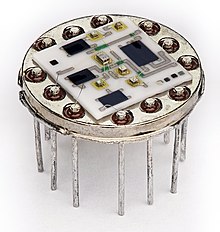
Hybrid integrated circuit (National Semiconductor LH033CG) in a variant of the TO-8 package with 12 leads

In electronics, TO-8 is a designation for a standardized metal semiconductor package. TO in TO-8 stands for "transistor outline" and refers to a series of technical drawings produced by JEDEC.[1] The TO-8 package is noticeably larger than the more common TO-5 package. While originally designed for medium power transistors (that is, higher power than TO-5 but lower than TO-3) such as the 2N1483 series[2] or the AD136,[3] it is more commonly used for integrated circuits and sensors (see Variants below).

Construction
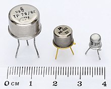
Size comparison between (left to right) TO-8, TO-5 and TO-18 packages

The typical TO-8 metal can package has a base diameter of 15.24 mm (0.600 in), a cap diameter of 12.29 mm (0.484 in), and a cap height of 7.62 mm (0.300 in).[1] The lead diameter is nominally 0.76 mm (0.030 in). The leads are arranged on a circle with a diameter of 7.16 mm (0.282 in). The minimum length of the leads is 10.16 mm (0.400 in).

Variants
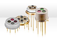
Left: sensor in a variant of the TO-8 package[4] with 8 leads and windows (right: TO-5 package variant for comparison)

Several variants of the original TO-8 package have the same cap dimensions but differ in the number and length of the leads (wires). Somewhat incorrectly, TO-8 is often used in manufacturer's literature as a synonym for any package with the cap dimensions of TO-8, regardless of the number of leads, or even for any package with the diameter of TO-8, regardless of the cap height and the number of leads. Light-sensitive or light-emitting devices have a transparent window, lens, or parabolic reflectors in the top of the case rather than a sealed, flat top.[4][5] There are variants with between 2 and 16 leads.[6] For packages with more than 4 leads, the leads are usually arranged along the edges of a square with a side length of 10.16 mm (0.400 in) (rather than on a circle as in packages with up to 4 leads or for other metal can packages such as TO-101).[7] These variants usually have a tab to identify lead number 1 and an increased cap diameter of 13.97 mm (0.550 in).[7]

National standards

TO-233 is intended to replace previous definitions of TO-8.[8][9]

Standards organization Standard Designation for
TO-8
JEDEC JEP95[9] TO-233-AA
IEC IEC 60191[a][10] C8/B13
DIN DIN 41878[3] 8A3
EIAJ / JEITA ED-7500A[a][11] TC-6/TB-7
British Standards BS 3934[a][10] SO-22/SB3-9
  1. ^ a b c These standards have separate drawings for the package case and the base.

References

  1. ^ a b "JEDEC TO-8 package specification" (PDF). JEDEC. Archived from the original (PDF) on 2016-04-10. Retrieved 2021-10-23.
  2. ^ "2N1483 – 2N1486". Microsemi. 2013. Retrieved 2021-10-23.
  3. ^ a b "Germanium PNP Transistor AD136 40V / 10A DATASHEET" (PDF) (in German). Siemens. Retrieved 2021-10-25.
  4. ^ a b "LMM-244-# Planar multi channel pyroelectric detector" (PDF). InfraTec. Retrieved 2021-10-25.
  5. ^ "Photodigm TO-8 Package". Photodigm. Retrieved 2021-10-25.
  6. ^ "TO-8 Package". EESemi. 2008. Retrieved 2021-10-25.
  7. ^ a b Larry Davis (2012-01-21). "Transistor Package Style 12-Lead TO-8 Can". interfacebus.com. Retrieved 2021-10-25.
  8. ^ "Index by Device Type of Registered Transistor Outlines (TO)". JEDEC Publication No. 95 (PDF). JEDEC. October 2010. Retrieved 2021-07-13.
  9. ^ a b "Header Family 0.280 Pin Circle" (PDF). JEDEC. 1976-06-01. Archived from the original (PDF) on 2016-04-10. Retrieved 2021-10-25.
  10. ^ a b "Semiconductors" (PDF). Pro Electron. 1978. pp. 215–221. Retrieved 2021-06-17.
  11. ^ "EIAJ ED-7500A Standards for the Dimensions of Semiconductor Devices" (PDF). JEITA. 1996. Retrieved 2021-06-14.
Prefix: a b c d e f g h i j k l m n o p q r s t u v w x y z 0 1 2 3 4 5 6 7 8 9

Portal di Ensiklopedia Dunia

Kembali kehalaman sebelumnya